Refresh of the FPGA Flash Memory Tester
fpga-serial-mem-tester-3
FPGA Serial Mem Tester Version 3
by Timothy Stotts
Now with support for:
- Digilent Inc. Arty S7-25 FPGA development board containing a small Xilinx Spartan-7 FPGA
- Digilent Inc. Arty A7-100 FPGA development board containing a large Xilinx Artix-7 FPGA
- Digilent Inc. Zybo Z7-20 APSoC development board containing a moderate Xilinx Zynq-7000 SoC.
Note that this project is kept as a intermediate-level design that students, hobbyists, and FPGA enthusiasts may find interesting.
Description
A small FPGA project of different implementations for testing a N25Q Serial Flash. Status is displayed in abbreviated text on a 16x2 character LCD, with color-mixing two or four RGB LEDs, and with displaying PASS and DONE status on two basic LEDs.
The Xilinx MicroBlaze designs can now target either of two FPGA development boards produced by Digilent Inc; one being lower cost. Also, the HDL design can target either of the same two FPGA development boards.
- Digilent Inc. Arty S7-25 FPGA development board containing a small Xilinx Spartan-7 FPGA
- Digilent Inc. Arty A7-100 FPGA development board containing a large Xilinx Artix-7 FPGA
Two peripherals are used: Digilent Inc. Pmod SF3, Digilent Inc. Pmod CLS.
Additionally, the Xilinx Zynq design targets the
- Digilent Inc. Zybo Z7-20 FPGA development board containing a Xilinx Zynq-7000 APSoC.
Two peripherals are used: Digilent Inc. Pmod SF3, Digilent Inc. Pmod CLS.
The design is broken into five groupings. The first group targets the Digilent Inc. Arty A7-100 development board. The second group targets the Digilent Inc. Arty S7-25 development board. The third and fourth groups target either the Digilent Inc. Arty A7-100 development board or the Digilent Inc. Arty S7-25 development board. The last group targets the Digilent Inc. Zybo Z7-20 development board. The projects are likely portable to the smaller Arty A7-35 and Zybo Z7-10, respectively as the designs are low resource utilization.
The folder SF-Tester-Design-MB-A7 contains a Xilinx Vivado IP Integrator plus Xilinx Vitis design. A MicroBlaze soft CPU is instantiated to talk with board components, a 16x2 character LCD display, and a N25Q serial flash. Source to be incorporated into a Xilinx Vitis project contain a small FreeRTOS program in C; drivers for the peripherals; and a main loop to execute a software FSM that operates byte-by-byte testing of the N25Q serial flash. This design targets the Arty A7-100 development board.
The folder SF-Tester-Design-MB-S7 contains a Xilinx Vivado IP Integrator plus Xilinx Vitis design. The design is essentially the same as the SF-Tester-Design-MB-A7 mentioned above, but instead targets the Arty S7-25 development board, including the differences in available board components, such as count of RGB LEDs.
The folder SF-Tester-Design-SV contains a Xilinx Vivado project with sources containing SystemVerilog 2012 RTL modules and VHDL visual test-bench. Plain HDL without a soft CPU or C code is authored to talk with board components, a N25Q SPI Flash 256Mbit, and a 16x2 character LCD peripheral. The design is essentially equivalent function as the SF-Tester-Design-MB-A7/SF-Tester-Design-MB-S7 projects, but executes much faster as the control loop FSM is implemented in hardware instead of a low-speed CPU. This design targets either of the Arty A7-100 or the Arty S7-25 development boards, and adjusts for the difference in available board components, such as count of RGB LEDs.
The folder SF-Tester-Design-VHDL contains a Xilinx Vivado project with sources containing only VHDL-2002 and VHDL-2008 modules. Plain HDL without a soft CPU or C code is authored to talk with board components, a N25Q SPI Flash 256Mbit, and a 16x2 character LCD peripheral. The design is essentially equivalent function as the SF-Tester-Design-MB-A7/SF-Tester-Design-MB-S7 projects, but executes much faster as the control loop FSM is implemented in hardware instead of a low-speed CPU. This design targets either of the Arty A7-100 or the Arty S7-25 development boards, and adjusts for the difference in available board components, such as count of RGB LEDs.
The folder SF-Tester-Design-Zynq contains a Xilinx Vivado IP Integrator plus Xilinx Vitis design. The Zynq hard ARM CPU #0 is configured to talk with board components, a 16x2 character LCD display, and a N25Q serial flash. Its functionality is mostly equivalent function to that of the SF-Tester-Design-MB-A7 design, but differs in the count of RGB LEDs.
HDL naming conventions notice
The Pmod peripherals used in this project connect via a standard bus technology design called SPI. The use of MOSI/MISO terminology is considered obsolete. COPI/CIPO is now used. The MOSI signal on a controller can be replaced with the title ‘COPI’. Master and Slave terms are now Controller and Peripheral. Additional information can be found here. The choice to use COPI and CIPO instead of SDO and SDI for single-direction bus signals is simple. On a single peripheral bus with two data lines of fixed direction, the usage of the signal name “SDO” is dependent on whether the Controller or the Peripheral is the chip being discussed; whereas COPI gives the exact direction regardless of which chip is being discussed. The author of this website agrees with the open source community that the removal of offensive language from standard terminology in engineering is a priority. Note that for CPU-based designs, the engineer cannot change the terminology in use by the tools.
Project Homepage
FPGA Serial Flash Memory Tester Version 3 project and source code
Project information document:
./Serial Flash Sector Tester - Refreshed.pdf
Serial Flash Sector Tester info
Diagrams design document (only the HDL designs):
./SF-Tester-Design-Documents/SF-Tester-Design-Diagrams.pdf
Serial Flash Sector Tester Design Diagrams info
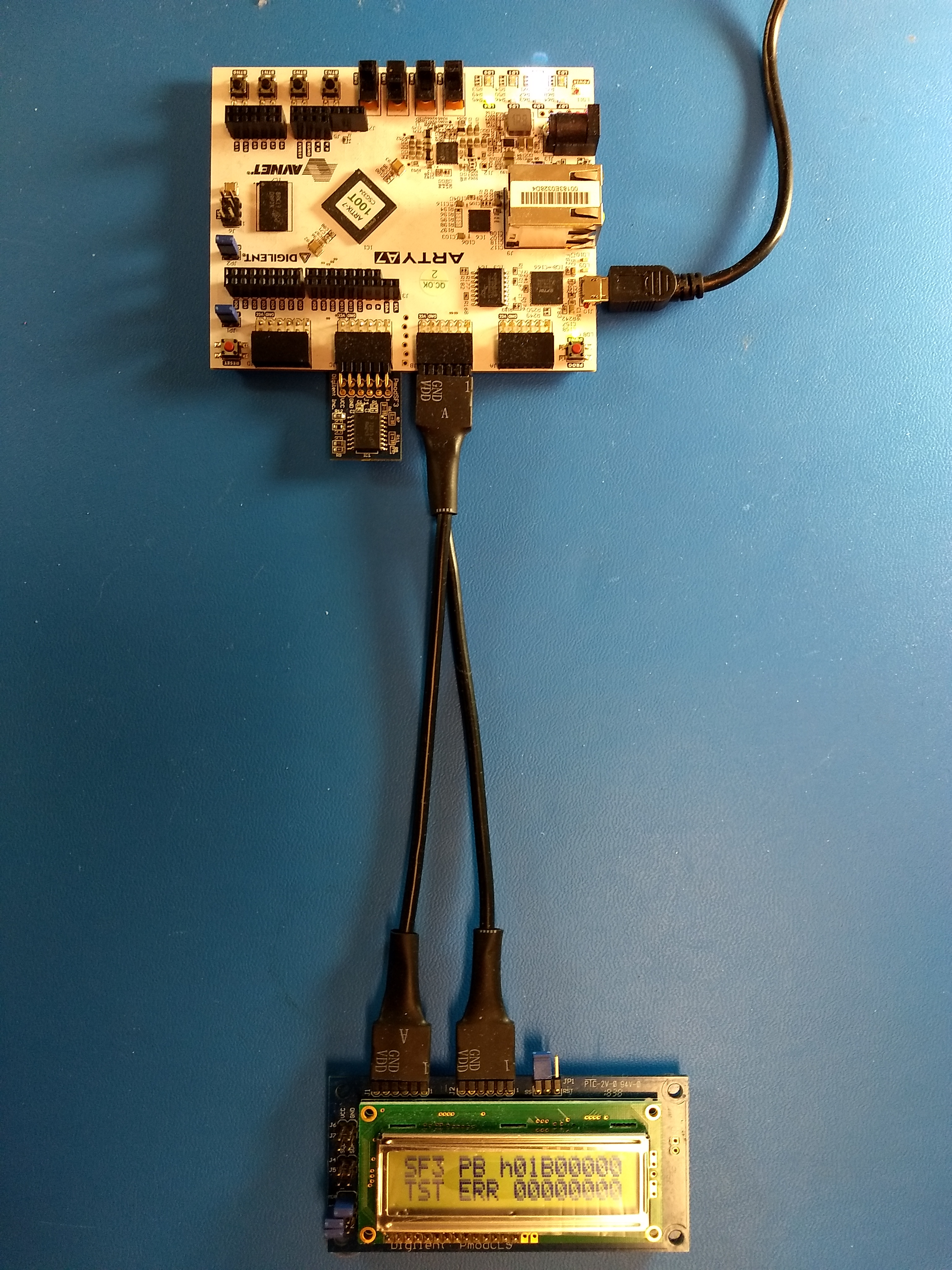
Target device execution: Arty A7-100 with Pmod SF3, Pmod CLS on extension cable
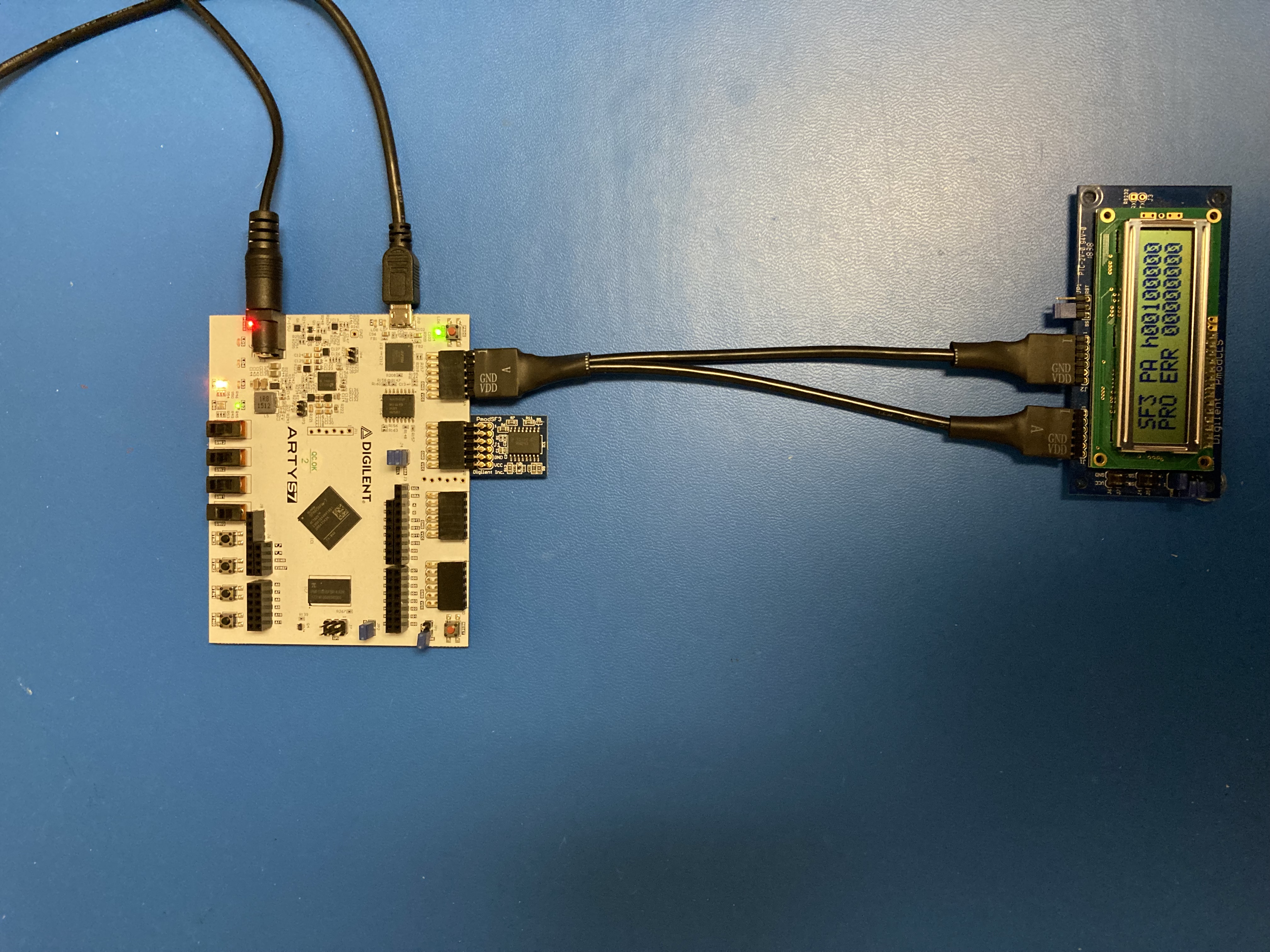
Target device execution: Arty S7-25 with Pmod SF3, Pmod CLS on extension cable
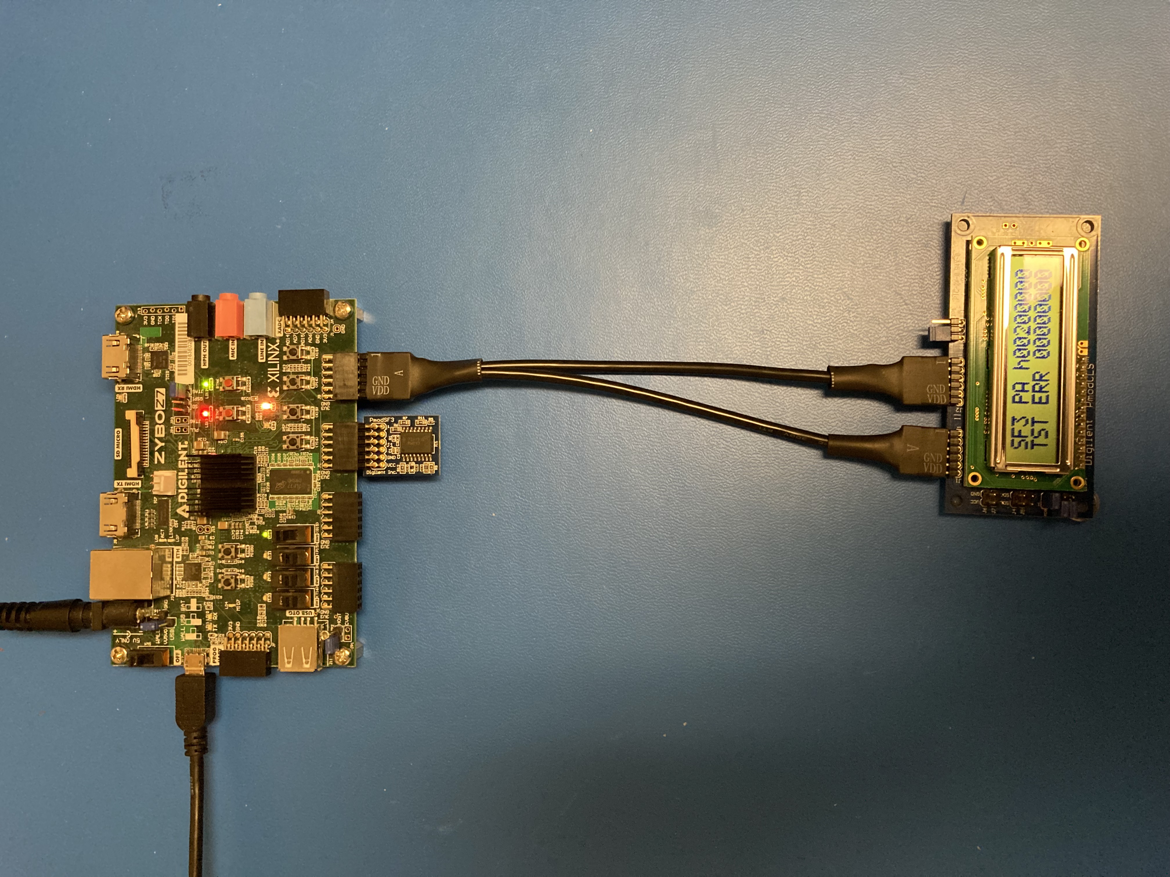
Target device execution: Zybo Z7-20 with Pmod SF3, Pmod CLS on extension cable
Block diagram architecture of the HDL design:

Top Port diagram architecture of the HDL design:
